PCB Assembly Process Flow Chart Circuit Diagram The PCB manufacturing process is a complex and multi-step journey that transforms a design concept into a functional electronic component. Each step, from design and material selection to final testing and inspection, plays a critical role in ensuring the production of high-quality, reliable, and efficient PCBs.
Learn how PCBs are designed, fabricated, and finished from schematic to delivery. Explore the different substrate materials, CAM software, and inspection methods used in the industry. Creating a PCB is a multi-step process that combines technology, precision, and quality control. There are twelve key steps when it comes to manufacturing a PCB. Design and Layout: The PCB design is created using specialized software where the position of each component, the traces, and any additional features like drill holes are planned out.
PCB Fabrication and Assembly Process Circuit Diagram
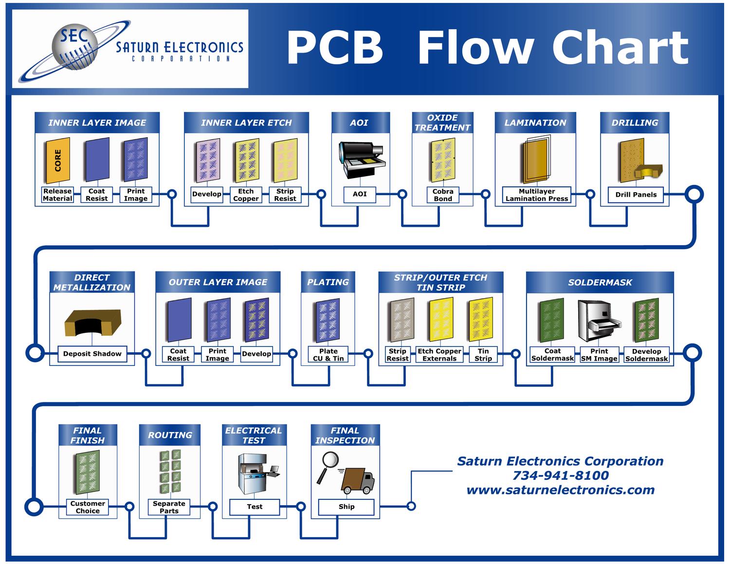
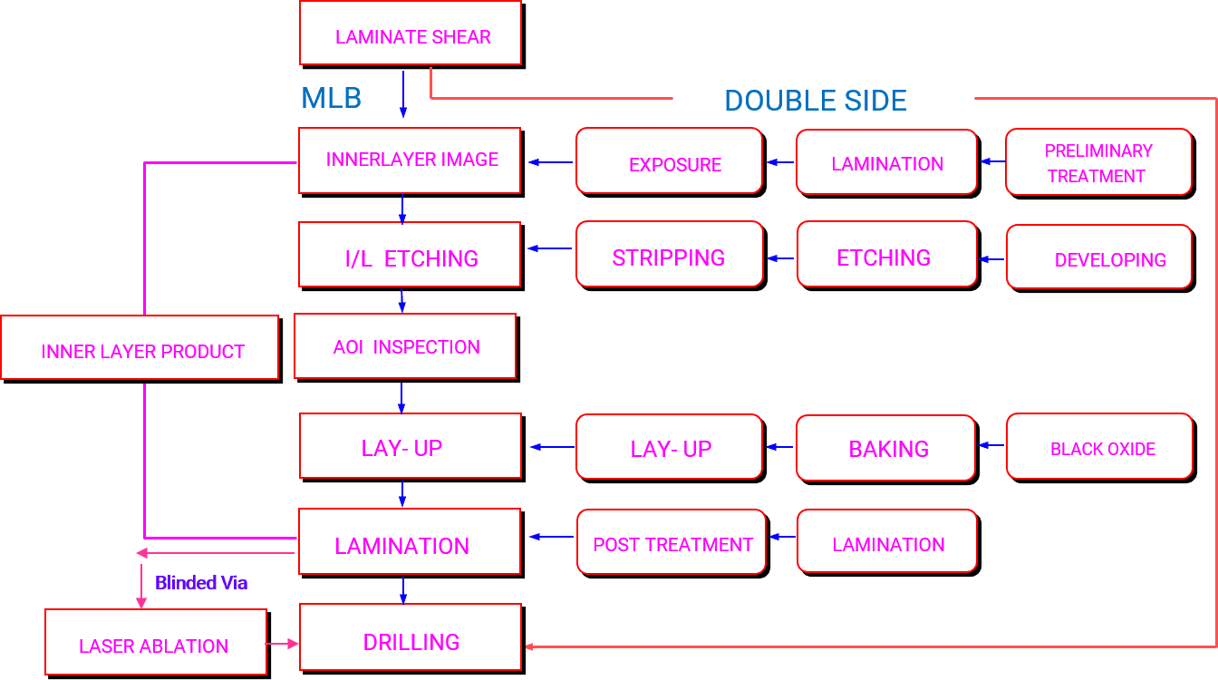
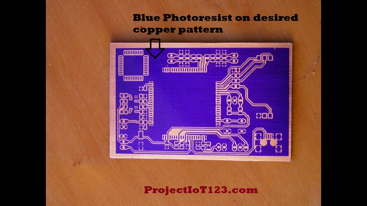
The process of PCB fabrication and assembly is very complex. Here is a step-by-step explanation of PCB fabrication and assembly, so you can easily understand the entire PCB fabrication and assembly process. PCB Fabrication. 1.Material. 2.Inner layer Exposure. 3.Inner Layers Dry film imaging.

The Step-by-Step PCB Fabrication Process . Preparing the Substrate: The Foundation of Every PCB The fabrication journey begins with selecting and preparing the substrate, typically a fiberglass-reinforced epoxy laminate like FR4. This substrate provides the mechanical structure and insulates the conductive pathways. The surface is cleaned Learn how PCBs are made from design to fabrication, and the different types of PCBs and their applications. Explore the history of PCB evolution and the parts of a PCB, such as substrate, copper layer, solder mask, and silkscreen.
PCB Manufacturing Process - A Step by Step Guide Circuit Diagram
Learn the steps involved in producing a printed circuit board (PCB) from design files to finished product. See photos and details of the processes for double-sided and multi-layer PCBs at Bay Area Circuits. Learn how PCBs are designed, printed, etched, drilled and plated in this comprehensive guide. See the details of each step, the tools and materials used, and the quality checks performed at each stage. Learn how PCBs are made with a detailed flowchart and video. Explore the steps of patterning, photoengraving, lamination, drilling, solder plating, silk screen and testing.